
Heavy Copper PCB Manufacturer in USA
At CircuiTek Solutions, we produce heavy copper printed circuit boards engineered to carry high current, withstand extreme temperatures, and deliver superior thermal performance. Heavy copper PCBs are used when standard copper thickness is no longer sufficient to meet electrical, mechanical, or heat dissipation requirements.
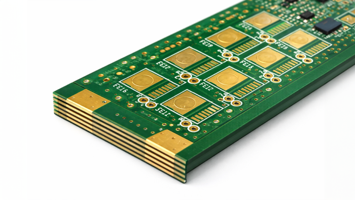
With finished copper thicknesses starting at 3 oz and extending up to 40 oz, heavy copper PCBs provide long-term durability and reliability in high-power applications.
What Is a Heavy Copper PCB?
A heavy copper PCB is a printed circuit board that incorporates significantly thicker copper layers than conventional PCBs. These boards are designed to support large current loads, elevated voltages, and harsh operating conditions while maintaining structural and electrical stability.
Heavy copper PCBs are commonly selected for applications requiring:
- High current-carrying capacity
- Efficient heat dissipation
- Extended service life
- Mechanical strength under stress
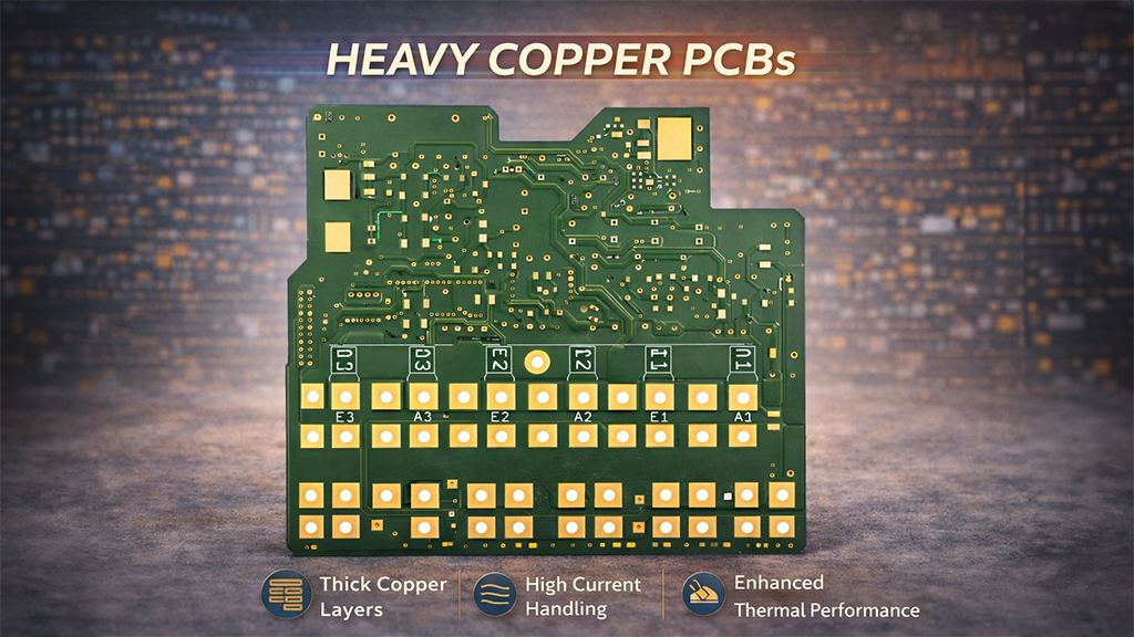
Key Features of Heavy Copper Printed Circuit Boards
As electronic systems continue to demand higher performance, heavy copper PCBs provide critical advantages over standard designs.
Key features include:
- High current and voltage handling
- Excellent thermal conductivity
- Enhanced mechanical durability
- Strong resistance to corrosion
- High electrical endurance
- Reliability in extreme environments
Materials Used in Heavy Copper PCB Manufacturing
Heavy copper PCBs are most commonly manufactured using High TG FR-4 materials, selected for their ability to tolerate heat and mechanical stress.
In multilayer heavy copper PCB construction:
- Manufacturing often begins with 2 oz base copper
- Electroplating is used to achieve finished copper thicknesses of 3 oz or greater
- Copper thickness is carefully controlled on both inner and outer layers
- Board thickness and layer count become critical design considerations
Selecting a qualified heavy copper PCB manufacturer in USA ensures proper material selection, copper distribution, and dimensional stability throughout fabrication.
Technical Characteristics of Heavy Copper PCBs
Heavy copper PCBs differ structurally and functionally from standard PCBs.
Thermal & Mechanical Resistance
These boards maintain performance across high and low temperature ranges without warping, cracking, or delamination.
Reinforced Plated Through-Holes and Vias
Increased copper thickness in via sidewalls and plated through-holes improves durability under high current and repeated thermal cycling.
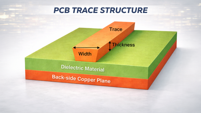
Electrical and Heat Dissipation Performance
Thick copper traces support large current flow while efficiently transferring heat away from sensitive components.
Advantages and Limitations of Heavy Copper PCBs
Advantages
Heavy copper PCBs provide:
- High reliability and extended product lifespan
- Superior current and voltage handling
- Excellent thermal conductivity
- Stable performance in harsh environments
Limitations
There are also important trade-offs:
- Not ideal for very high-density trace designs
- More complex manufacturing processes
- Higher cost compared to standard PCBs
Tighter design and fabrication tolerances
Applications of Heavy Copper Printed Circuit Boards
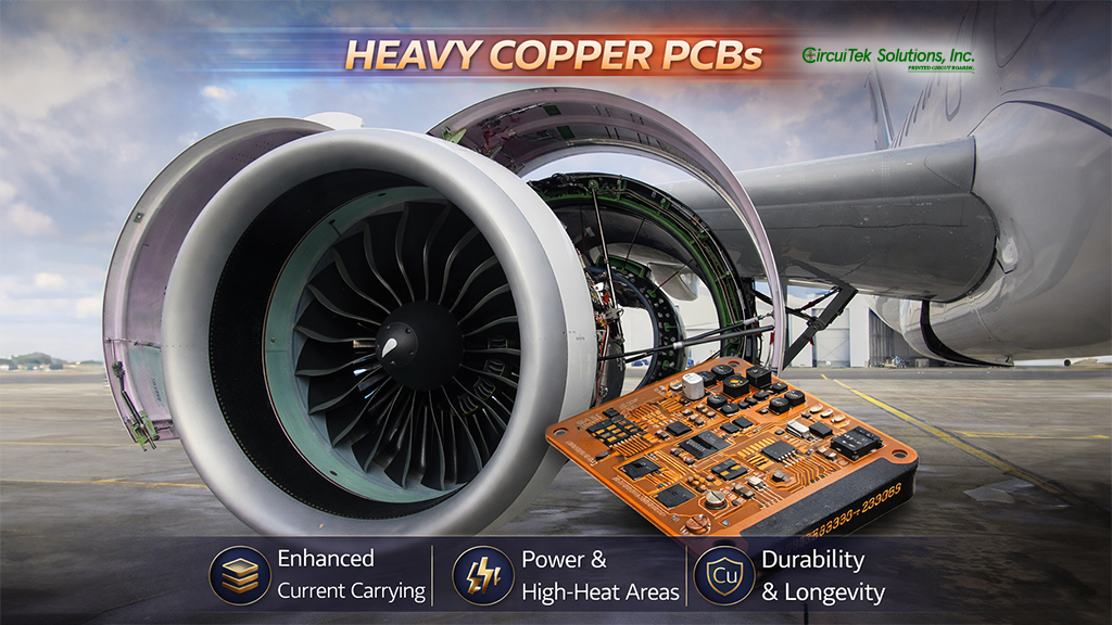
Heavy copper PCBs are widely used in applications requiring high power and durability, including:
-
Power supply units
and power converters
-
Aerospace and satellite
communication systems
-
Network base
stations and infrastructure
-
Hybrid integrated circuits and
control modules
-
Automotive
and industrial power electronics
-
Medical
and diagnostic equipment
-
RF
and microwave systems
-
High-power consumer
and home appliances
Why Choose Circuitek Solutions Inc. for Heavy Copper PCB Manufacturing?
Circuitek Solutions Inc. is a trusted heavy copper PCB manufacturer in USA, delivering custom printed circuit boards built to precise specifications and industry standards.
We specialize in:
- Quick-turn manufacturing
- Prototype to high-volume production
- 2–40 layer PCB constructions
- Via-in-pad (conductive, non-conductive, copper-plugged)
- Heavy copper circuit designs
- Controlled impedance PCBs
- ENIG surface finish
- ENEPIG surface finish
- Hard Gold Fingers
- Wire-bondable electrolytic gold
- Immersion Tin
- Immersion Silver
- HASL
- Lead-Free HASL (LF HASL)
Our engineering-driven manufacturing process ensures consistent quality, durability, and performance across demanding environments.
EEAT-BASED & SEARCH-DRIVEN
A PCB is typically considered heavy copper when the finished copper thickness exceeds 3 oz per layer, with some designs reaching 20–40 oz depending on application needs.
Heavy copper PCBs are recommended for designs that require high current capacity, improved heat dissipation, or long-term reliability in extreme operating environments.
Yes. Heavy copper PCBs can be produced as multilayer designs, though careful planning is required to manage copper distribution, board thickness, and thermal performance.
Industries such as aerospace, automotive, industrial power electronics, telecommunications, medical devices, and energy systems benefit most due to their high-power requirements.