
PCB Design & Engineering Services
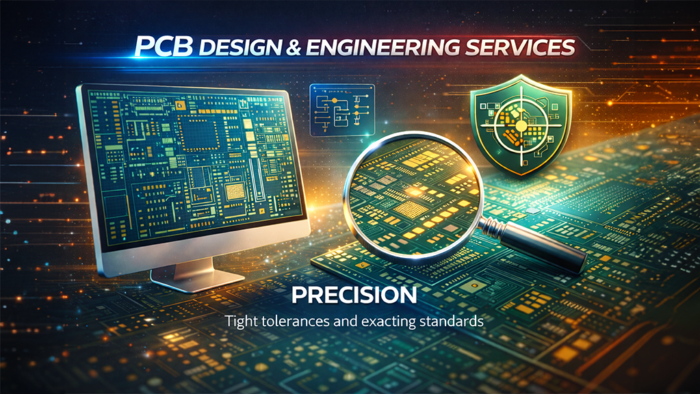
Great PCB performance starts long before fabrication. Our PCB design and engineering services bridge the gap between concept and production by transforming early-stage ideas into manufacturable, reliable circuit board designs.
We work directly with engineers, product developers, and OEM teams to ensure each board layout is optimized for fabrication, assembly, electrical performance, and long-term reliability — not just theoretical functionality.
Turning Design Concepts into Manufacturable Boards
A PCB design that works on paper can still fail in production if manufacturability is not considered early. Our design support focuses on real-world fabrication and assembly constraints, helping prevent redesigns, delays, and unexpected cost increases.
We support designs at every stage, including:
- Early concept validation
- Pre-layout engineering guidance
- Design refinement before fabrication
- Production readiness checks
This approach ensures your board is not only functional, but buildable at scale.
Engineering Support Throughout the Design Process
Our engineering team supports PCB designs with a manufacturing-first mindset. We collaborate closely to align electrical requirements with fabrication realities.
Engineering support includes:
- Design feasibility evaluation
- Material selection guidance
- Layer count optimization
- Thermal and mechanical considerations
- Reliability and lifecycle planning
By addressing these factors early, we help reduce risk and improve first-pass success.
Design for Manufacturability (DFM) Review
DFM review is a critical step in preventing production issues. Our PCB DFM review process identifies potential risks before fabrication begins.
DFM review focuses on:
- Trace width and spacing compliance
- Via structures and drill limitations
- Annular ring and pad sizing
- Soldermask and silkscreen alignment
- Assembly compatibility and tolerances
These reviews help eliminate costly rework and improve yield during fabrication and assembly.
Stack-Up Development and Material Selection
Proper stack-up design is essential for signal integrity, impedance control, and mechanical stability. We develop stack-ups tailored to your electrical and manufacturing requirements.
Stack-up development includes:
- Layer count planning
- Dielectric selection
- Copper weight optimization
- Controlled impedance routing support
- Compatibility with fabrication processes
Each stack-up is engineered to balance performance, reliability, and cost.
Impedance Calculations and Signal Integrity Support
High-speed and high-frequency designs require precise impedance control. We support impedance-controlled PCB design by aligning layout geometry with material properties and fabrication tolerances.
Impedance support includes:
- Single-ended and differential impedance calculations
- Trace width and spacing optimization
- Reference plane alignment
- Signal return path evaluation
- High-speed and RF design considerations
This ensures signals perform as intended across operating conditions.

File Optimization and Production-Ready Outputs
Even well-designed boards can be delayed by incomplete or misaligned files. We optimize and validate all design outputs to ensure smooth handoff to fabrication and assembly.
File optimization includes:
- Gerber and ODB++ validation
- Drill file review and alignment
- Netlist verification
- Panelization considerations
- Manufacturing notes and documentation
The result is a clean, production-ready design package that minimizes questions and turnaround time.
Supporting Prototypes Through Production
Our design services support both prototype development and scalable production. Whether you are validating a new concept or preparing for volume manufacturing, we help ensure your design transitions smoothly.
We support:
- Prototype design refinement
- Low-volume pilot builds
- Design adjustments for scale
- Ongoing engineering collaboration
This continuity reduces redesign cycles and accelerates time-to-market.
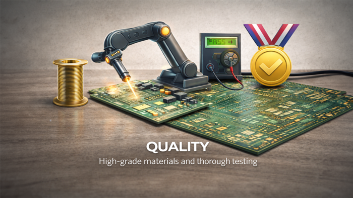
Why Choose Circuitek Solutions Inc. for PCB Design Support?
Our PCB design and engineering services are backed by real manufacturing experience. Every recommendation is grounded in how boards are actually fabricated, assembled, and tested.
We provide:
- Manufacturing-driven design insight
- Clear engineering communication
- Practical, buildable solutions
- Support across diverse PCB technologies
- Alignment with IPC standards and industry best practices
This ensures your design is ready not just to function — but to be built reliably.
EEAT-BASED & SEARCH-DRIVEN
DFM ensures a PCB layout can be fabricated and assembled reliably by aligning design choices with manufacturing capabilities and tolerances.
DFM review should occur before fabrication, ideally after layout completion but before files are released for production.
Stack-up design affects impedance, signal integrity, thermal behavior, and mechanical stability, making it critical for reliable performance.
Yes. Early engineering and DFM review help prevent redesigns, reduce scrap, improve yield, and shorten production timelines.