
PCB Manufacturing & Production Process
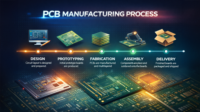
Reliable PCBs are built through discipline, documentation, and control — not shortcuts. Our PCB manufacturing process follows a structured, step-by-step production workflow that ensures consistency, traceability, and quality from engineering review through final shipment.
Every board is fabricated using a fully documented process designed to reduce risk, improve yield, and deliver repeatable results across prototype, low-volume, and production builds.
A Controlled Manufacturing Workflow from Start to Finish
Our production process is designed to eliminate uncertainty. Each stage of fabrication follows defined procedures, verification checkpoints, and documented outputs to ensure every board meets specification before advancing.
The manufacturing workflow includes:
- Engineering validation
- Material preparation
- Layer lamination
- Drilling and PTH process
- Plating and surface finishing
- Testing and final inspection
- QC check and documentation
- Packaging and shipment
This structured approach ensures process stability and repeatability.
Engineering Review Before Fabrication
Every production run begins with an engineering review to confirm manufacturability and alignment with specifications. This step ensures the design can be built reliably before materials are committed.
Engineering review includes:
- File verification and Pre-engineering
- Stack-up confirmation
- Material and copper weight validation
- Drill and via structure review
- Tolerance and capability alignment
- Netlist testing parameters
- Complete DRC and DFM checks
- Solving engineering queries by customer communication
- Finalize data for fabrication
This step prevents production delays and downstream defects.
Material Control and Preparation
Material quality directly impacts board performance and reliability. All laminates, copper foils, prepregs, and specialty materials are verified and prepared according to documented procedures.
Material control includes:
- Material traceability and lot tracking
- Storage and handling controls
- Thickness and copper verification
- Compatibility with stack-up requirements
This ensures consistency across builds and repeat orders.
Imaging, Etching, and Layer Formation
Circuit layers are created using controlled imaging and etching processes to achieve precise trace geometry and spacing.
Layer formation includes:
- Photo-imaging and exposure control
- Precision etching for trace accuracy
- Inner layer inspection and verification (AOI)
- Registration alignment checks (X-ray)
These steps ensure electrical performance and dimensional accuracy using high tech fully automated machinery.
Lamination, Drilling, and Via Formation
Lamination and drilling define the structural integrity of the PCB. These steps are executed under tightly controlled conditions to maintain alignment and reliability.
Key processes include:
- Multilayer lamination under controlled pressure and temperature
- Mechanical and laser drilling
- Via formation and wall preparation
- Registration verification
This phase is critical for multilayer, HDI, rigid-flex, and impedance-controlled boards.
Plating and Surface Finishing
Plating processes establish electrical connectivity and durability. Surface finishes are applied based on functional and environmental requirements.
Plating and finishing includes:
- Through-hole and via plating
- Copper thickness control
- Surface finishes such as ENIG, ENEPIG, Immersion Silver, HASL, or Hard Gold
- Thickness and adhesion verification
Each finish is selected and applied to meet performance and lifecycle needs.
Solder Mask, Legend, and Final Processing
Protective and identification layers are applied to ensure assembly reliability and traceability.
Final processing includes:
- Solder mask application and curing
- Legend and marking accuracy
- Routing, profiling, and depanelization
- Dimensional verification
These steps ensure boards are assembly-ready.
Inspection, Electrical Testing, and Quality Control
Quality control is built into every stage of production, with final verification before shipment.
Quality assurance includes:
- Automated Optical Inspection (AOI)
- Electrical testing (flying probe)
- Visual inspection
- Process documentation and reporting
All results are recorded to maintain accountability and traceability.
Documentation, Traceability, and Compliance
Every production run is supported by documentation that tracks the board from raw material through shipment.
Documentation includes:
- Process travelers
- Inspection and test records
- Material traceability
- Compliance verification
Reports preparation- FAI, C of C, Test report, Material Certifications and others.
This documentation supports audits, repeatability, and long-term supply chain confidence.

Packaging and Shipment
Boards are packaged to prevent damage, contamination, and environmental exposure during transit.
Shipment preparation includes:
- Protective packaging
- Moisture barrier handling when required
- Labeling and documentation
- Coordinated delivery timelines
This ensures boards arrive ready for assembly.
Why Choose Circuitek Solutions Inc. for PCB Manufacturing?
Our manufacturing process is built around control, documentation, and accountability, not volume shortcuts.
We provide:
- Fully documented production workflows
- Consistent process control
- Manufacturing transparency
- Support from engineering through delivery
- Scalable production from prototype to volume
This approach ensures your boards are built right the first time — and every time.
PROCESS & QUALITY FOCUSED
A controlled process ensures consistency, reduces defects, and supports traceability across production runs.
Yes. Engineering review is a required first step to validate manufacturability before fabrication begins.
Quality is verified through inspection checkpoints, AOI, electrical testing, and documented verification.
Yes. The same controlled workflow is applied to prototypes, pilot builds, and full production runs.