
HDI PCB Manufacturer in USA
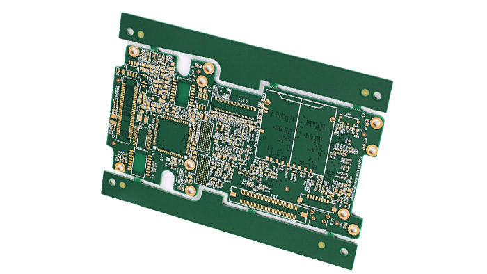
High-density interconnect PCB manufacturing at CircuiTek Solutions focuses on producing high-density interconnect printed circuit boards engineered for compact, lightweight, and high-performance electronic devices. As electronic systems continue to shrink while performance demands increase, HDI PCB technology allows designers to integrate complex functionality into smaller footprints without sacrificing reliability. According to IPC standards, HDI designs incorporate advanced microvia structures and fine-line routing to support modern electronic requirements.
HDI PCBs support advanced routing, fine features, and specialized via structures that are not achievable with conventional designs, including blind and buried vias, stacked microvias, and high layer counts. These capabilities enable improved signal integrity, reduced signal loss, and increased component density, making HDI PCBs ideal for applications such as medical devices, aerospace systems, telecommunications equipment, and high-speed digital electronics. Our PCB design engineering team works closely with clients to ensure proper stack-up configuration, impedance control, and manufacturability.
As part of our integrated PCB manufacturing process, HDI production requires precision fabrication techniques, strict process control, and advanced inspection methods to ensure consistent quality. These boards can be fully supported through our PCB assembly services, allowing for seamless transition from design through production. For applications requiring additional performance characteristics, HDI designs are often paired with technologies found in high-speed PCB and RF and microwave PCB solutions.
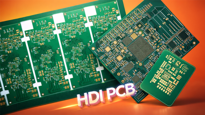
What Is an HDI PCB?
HDI PCB (High-Density Interconnect) technology refers to printed circuit boards engineered with microvias, fine trace widths, tight spacing, and sequential lamination to support high component density. These advanced structures require precision fabrication methods that go beyond traditional PCB manufacturing processes, allowing for more complex routing within smaller board footprints.
As electronic devices become smaller and more complex, HDI PCB designs enable improved electrical performance, reduced signal loss, and increased functionality without increasing overall board size. These capabilities are often integrated with advanced PCB design engineering practices to ensure proper stack-up configuration, signal integrity, and manufacturability in high-performance applications.
HDI PCBs typically include:
- Laser-drilled microvias
- Blind and buried vias
- Fine line and spacing geometries
- Sequentially laminated layer structures
These features allow advanced interconnections in compact designs.
Key Features of HDI Printed Circuit Boards
HDI PCB technology introduces capabilities that exceed traditional PCB fabrication limits.
Key features include:
- Multi-layer constructions starting at 4 layers
- Common stackups ranging from 6 to 12 layers or more
- High-precision fine line and spacing technology
- Advanced via structure for dense routing
These features allow designers to maximize functionality while minimizing board size and weight.
Materials Used in HDI PCB Manufacturing
High-density interconnect PCBs require materials that support fine features, thermal stability, and long-term mechanical reliability. HDI PCB materials are carefully selected for their high glass transition temperature (Tg), low coefficient of thermal expansion (CTE), excellent laser drill performance, low dielectric loss, and strong copper adhesion. These properties are critical for maintaining structural integrity and signal performance in compact, high-density designs.
To achieve the precision required for advanced routing, HDI PCB materials must also support ultra-thin dielectric layers used in microvias and fine-line circuitry. These capabilities go beyond traditional PCB manufacturing processes and require specialized material systems and fabrication techniques. In many applications, HDI designs are paired with materials found in high-speed PCB and high-Tg PCB solutions to ensure consistent electrical performance under demanding conditions.
Common HDI materials include:
- High-TG FR-4 (170 TG)
- IT-180A and ITEQ IT-180
- Isola 370HR
- Ventec VT-47
- Polyimide materials
- Panasonic (Megtron series)
- Nelco (N7000-2HT)
- Rogers Corporation (4000 series)
Material selection depends on signal integrity, thermal demands, and application environment.
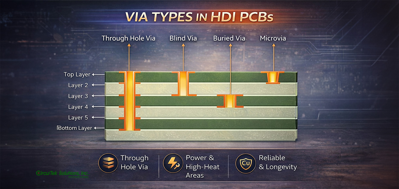
Via Technologies Used in HDI PCBs
HDI PCB fabrication relies on specialized via structures to support dense interconnections.
Common via types include:
- Microvias (laser-drilled, typically 4 mil or smaller)
- Blind vias connecting outer to inner layers
- Buried vias connecting internal layers only
- Stacked vias aligned vertically across layers
- Staggered vias offset step-by-step for multi-layer connections
- Sequential lamination structures enabling complex interconnects
Sequential lamination allows copper and dielectric layers to be added in stages, enabling highly complex HDI constructions.
Technical Characteristics of HDI Printed Circuit Boards
HDI PCBs are defined by several advanced structural characteristics.
High Wire Density
Dense routing allows more connections within a smaller area, enabling compact and lightweight devices.
Microvia Integration
Laser-drilled microvias reduce signal path length and improve electrical performance.
Fine Traces and Spacing
Trace widths as small as 2 mil with spacing near 3 mil enable increased routing density.
Electrical Performance
Shorter signal paths reduce signal distortion, crosstalk, and delay.
Advantages of Using HDI PCBs
HDI PCB technology delivers measurable performance and manufacturing benefits.
Advantages include:
- Improved electrical performance and reliability
- Smaller board size with higher functionality
- Faster signal transmission with reduced loss
- Reduced material usage compared to multi-board designs
- Efficient component placement on both sides of the board
Cost optimization at scale through design consolidation
Applications of high-density interconnect Printed Circuit Boards
HDI PCBs are widely used in industries that demand compact, high-performance electronics.
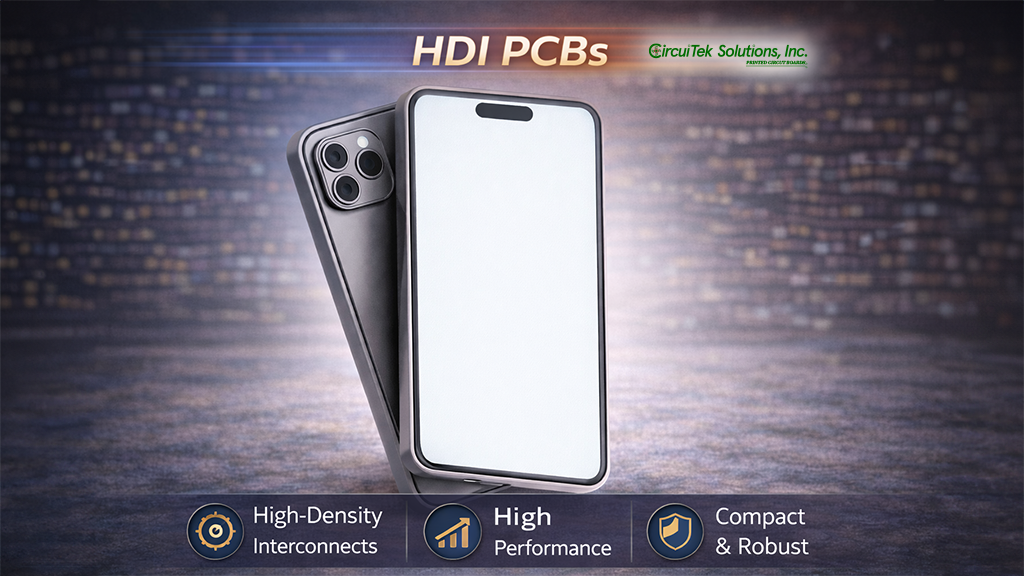
Applications include:
-
Smartphones, tablets
wearables, and AR/VR devices
-
Defense and aerospace
systems
-
Communications and networking
equipment
-
Automotive control units
and infotainment systems
-
Medical devices
and robotic surgical tools
-
High-performance
consumer electronics
Why Choose Circuitek Solutions Inc. for HDI PCB Fabrication?
Circuitek Solutions Inc. is a trusted high-density interconnect PCB manufacturer in USA, delivering custom HDI solutions built to exact specifications.
We specialize in:
- Quick-turn prototyping
- Prototype to mid- and high-volume production
- Advanced HDI stackups and via structures
- Precision microvia drilling and lamination
- Domestic and offshore manufacturing options
- Competitive pricing with engineering support
Our manufacturing processes are engineered to meet the demands of modern high-density electronics.
FAQ SECTION
High-density interconnect PCBs use microvias, fine traces, and sequential lamination to achieve higher routing density and better electrical performance than conventional PCBs.
HDI technology is recommended when space is limited, component density is high, or signal integrity requirements exceed the capabilities of standard PCBs.
High-density interconnect PCBs can have higher fabrication costs due to advanced processes, but they often reduce overall system cost by consolidating multiple boards into one.
Industries such as consumer electronics, automotive, aerospace, defense, medical devices, and telecommunications rely heavily on high-density interconnect PCB for compact, high-performance designs.