What is a HDI PCB?
Now a days, all the electronic components are getting compact and lightweight yet demanding ever improving performance. To accommodate this, you need to pack all the complex functionality into a smaller area, there comes HDI (High-density interconnect) PCB. The smaller the equipment gets, the more likely it is to employ HDI technology. Circuitek Solutions Inc., being a trusted hdi printed circuit board supplier, provides innovative solutions for these advanced requirements.
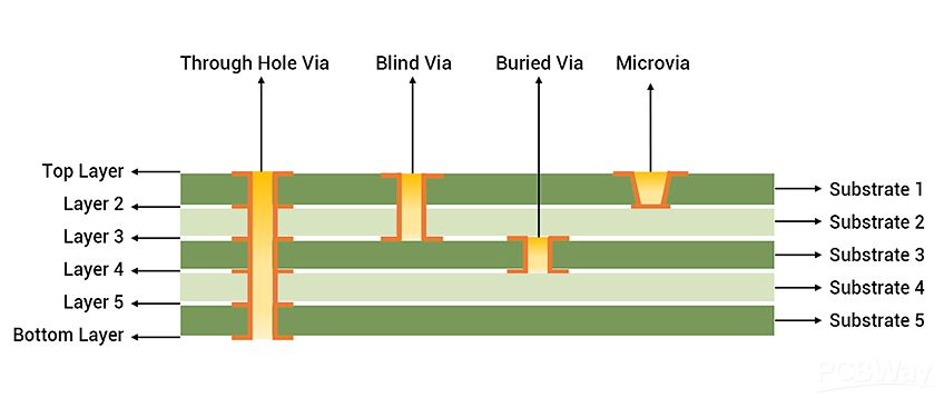
As the picture shows, HDI PCB is packed with the features like micro vias (laser drill starting from 4 mil size), combination of buried and blind vias, fine line and spacing, with the sequential lamination constructions etc.


What are the main features of HDI PCBs?
-
Layer counts:
Usually, an HDI PCB starts with 4 layers, but they are designed with very complex technology to accommodate features like tiny traces, micro vias, fine traces, and typical construction, they range from 6 layers to 12 layers or more. As an experienced hdi pcb manufacturer, we specialize in multi-layer HDI board fabrication.
-
Fine lines and spacing:
Due to the compactness of the electronic devices, the trace width and spacing on the HDI PCB needs to be designed as small as possible (4 mil or less)
-
Drill technology:
High density interconnect PCBs have various types of via technology based on the layer stack up and the build-up of the vias that plays a vital role. Micro via, blind via, and buried via are the different types of vias that are used instead of through-hole vias. Metallization and stacking up are the processes to ensure that the via is void-free hence maintains a low aspect ratio.
- Micro via - Micro via is a via size drilled 4 mil with laser technology.
- Buried via - Buried via are the drills buried in the middle layers that we cannot see them.
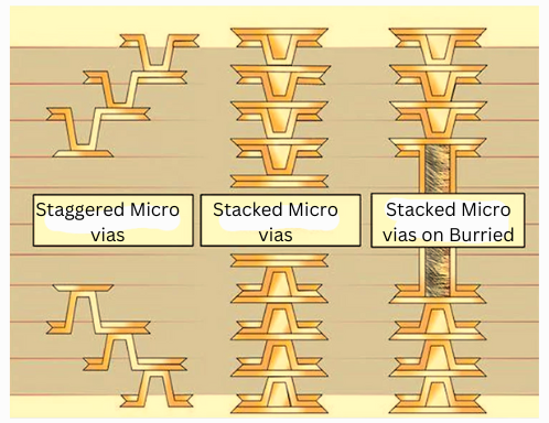
- Stacked via - Stacked via are the multiple vias placed directly on top of each other with connections between multiple layers.
- Staggered via - staggered via are the via structure used to connect three or more layers and are offset step by step within a single row on top of each other.
- Sequential lamination - Sequential lamination plays a vital role on HDI PCB fabrication where copper layers and insulating materials are stacked and laminated in a series of steps, that creates a complex, high-density interconnect (HDI) PCBs allowing the features like blind, buried and other types of vias generation. The thickness of HDI PCB is usually more than the regular PCB so to adapt the drill technology.
What materials are used to build HDI PCBs?
Several materials can be used for HDI PCB production including FR-4 (170-tg), IT-180A, ITEQ IT-180, Isola 370HR, Ventec VT-47, Polyimide etc. depending upon the technology requirements of the product.
What are the technical aspects, structure, and characteristics of HDI PCB?
The complex and dense design of the HDI PCB has the following aspects and characteristics: High wire density: smaller area and dense design leads to accommodating more components and connections results lighter and compact devices.
-
Micro via technology:
different via type combines in a single structure greatly helps the HDI Technology. The smallest laser drill is of 0.004".
-
Tiny traces and small spaces:
The complex design of 2 mil thick traces and 3 mil space between them enables to pack more connections in a limited space results miniaturization of the device with higher functionality.
-
Performance:
The improved electrical performance in the HDI PCB is due to the shorter signal path and reduced signal distortion.
-
Compact Design:
The key advantage of the complex design in a smaller space accommodating more components resulting in the smaller and lighter devices.
-
Sequential lamination:
The special structural development of HDI PCB includes 1+N+1 HDI structure, 2+N+2 HDI structure, 3+N+3 HDI structure, 4+N+4 HDI structure, i+N+i structure, Any layer connection
(where "N" means the number of core layers and the additional layers are used for via stacking and interconnections in the lamination)
-
Interconnect Via Structures:
The HDI Printed Circuit Board has advanced via design that includes regular through holes, blind via, buried via, stackable via, staggered via etc. All these comprise a more complex routing of the signal lines.
Reduced or fewer Layer Count: Compact design, thinner PCB, the via technology, tiny traces, special lamination of the HDI PCB helps the design having less layer counts than the conventional PCB.
-
Manufacturing Challenges:
HDI PCB manufacturing requires advanced and sophisticated machines, skilled workers, advanced production planning, and specialized process equipment. Being a leading hdi pcb manufacturer, we pride ourselves on overcoming these challenges effectively.
What are the advantages of using HDI PCBs?
The exceptional characteristics of High TG materials advantages the device working at its normal due to:-
Performance and reliability:
Compact and complex technology of HDI PCB enhances improved electrical performance by collaborating quick signal transmission with reduced signal loss and crossing delays, all the features packed in a small sized device yielding higher performance with greater reliability.
-
Small size and low Weight:
HDI PCB has compact size and light weight with facility of having components mounting on both the sides benefits usage of a small space that expands the capability of the equipment enabling functionality.
-
Faster production times keep you ahead in the market:
The High-Density Interconnect PCB design technology replaces multiple traditional boards utilizing less space and less materials with easy to mount and test components on either side saves a lot of time in manufacturing which enables faster electronic manufacturing facilitates you to lead the market.
Once on a traditional device requiring multiple PCBs, the HDI PCB technology replaces those multiple boards on a single PCB with high reliability and greater performance in a smaller area and less material utilization. This feature ultimately is a cost effective adding value to your project.
The superior technology of the High-Density Interconnect PCB has the arrangement of micro vias with their relative layer stacking enables performance and reliability of the modern electronics that yields satisfied customers.
What are the different applications of HDI PCB?
Commercial Products
The HDI PCBs play a major role in devices which operate at a high performance with high-definition displays. The devices like mobile phones, tablets, smartwatches, augmented reality, and Virtual Reality are some of the examples.
Defense and Aerospace
The HDI PCB serves high tech Defense and Aerospace systems which use high power and highly sensitive devices with precise data and communication systems and a compact size and light weight is an added benefit.
Communications
In any electronic communications devices using radio frequencies like routers, switches, panels, modules, networking devices etc. there is a good chance they pusses HDI PCB functioning well inside. Also, the audio video equipment is a part of it.
Automotive Applications
The vehicle control units, high speed microprocessors, vehicle displays, high density routing, telematic and computing systems all these crucial parts that drive today’s automotive require a compact and highly reliable technology. HDI PCB is a main part of it.
Healthcare and Medical Devices
The medical industry follows strict standards and more stringent rules for validation, all the machines need to be precise and safe. The lifesaving medical tools that are used in robotic surgery with tiny devices like colonoscopy, precision small camaras and lots of other devices use High-density interconnects PCB. Also, the laser operating machines in the ophthalmic industry are digitally controlled using High-Density Interconnect PCBs.
Consumer Electronics
In today’s modern era, all the high-tech wearables, tables, smartphones, camara, and lot of other devices operate on a powerful technology that is backed by the HDI PCB.
Why choose Circuitek Solutions Inc. for HDI PCB fabrication?
Each custom HDI PCB we deliver is supported by perfectly planned engineering and tailored manufacturing to ensure functionality and reliability. Whether you need a prototype or mid-to-high volume production, Circuitek Solutions Inc. — a trusted hdi printed circuit board supplier and hdi pcb manufacturer — is ready to support you with fast quotes, domestic and offshore manufacturing, competitive prices, and excellent service.
Also take advantage of our ongoing“50% off on tooling cost” offer for your first five orders.