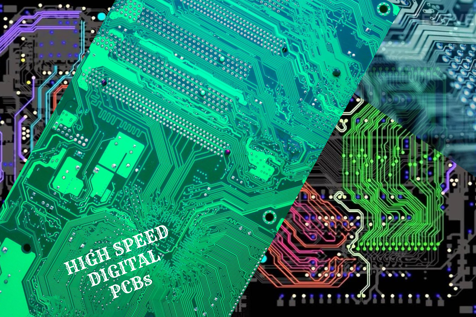
What is a High Speed Digital PCB?
High Speed PCBs are specially designed to transmit and receive signals at high frequencies. These types of PCBs are commonly used in electronic devices such as computers, smartphones, routers, and other high-speed data communication systems. As a leading high speed PCB supplier, we understand that the signal densities of high speed digital PCBs run into a few GHz. (50 MHz or more). The High Speed Digital PCB requires special consideration for signal integrity, power integrity, and EMI/EMC issues (EMI—unwanted electronic energy that disrupts device performance / EMC—the ability of the system to work as intended in its electromagnetic environment).
What are the main features of High Speed Digital PCB?
To minimize noise and interference, maintaining proper impedances with signal integrity is the main feature of the High Speed Digital PCB. As a trusted high speed PCB manufacturer, we ensure the following detailed key features are well-implemented:
-
Impedance Control:
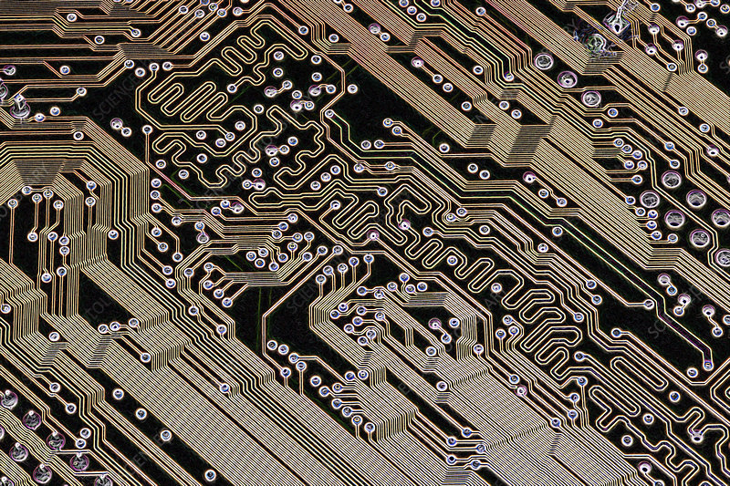
High-speed as well as differential signals have specific impedance requirements, which can cause reflections and signal degradation if the routing is not proper. A characteristic impedance is the ratio of amplitudes of voltage and current of a single wave propagating on a transmission line. For characteristic or surge impedance, the impedance of one transmission line must not affect the other. The impedance value of a transmission line is hence calculated in isolation without considering the impact of other lines. If you require a routing space of 5 to 6 layers, the actual PCB design must have ten layers for efficient impedance control.
-
Differential Signaling:
Differential signaling, a method widely adopted by any top high speed PCB supplier, uses two complementary signals instead of one, minimizing noise and ensuring minimal skew between signals.
-
Signal Integrity:
Signal integrity is highly essential for high-speed digital PCBs for maintaining high-frequency signals. It assures that the signal will reach the destination without any distortion. Signal integrity can be achieved by minimizing signal reflections, maintaining proper impedance control, and taking measures in the design to prevent crosstalk.
-
Return Paths:
High-speed signals require a low impedance return path to complete the circuit. There must be enough uniform ground for efficient routing. There must be minimal or no gaps between ground planes and power planes, as the routing of high-transmission lines through these gaps is challenging.
-
Thermal Management:
High-speed circuits generate excessive heat, which can degrade signal performance and damage components. Proper thermal management, such as heat sinks, is essential to ensure the reliable operation of high-speed PCBs.
-
Simulation and Analysis:
Proper simulation tools are essential during the design process to model circuit behavior and identify potential issues, something every expert high speed PCB manufacturer in USA must prioritize.
What materials are used to build High Speed Digital PCB?
High Speed Digital PCB required a special material that has certain properties to handle dielectric constant, thermal expansion coefficient (CTE), and loss tangent or dissipation with heat resistance, mechanical toughness, good (reliability) with stable Dk /Df parameters, with low roughness of the copper foil surface is recommended.
Several materials like FR-4 (170-tg), Isola High Performance like Tachyon, I-Speed, FR408HR, Rogers (RO3203, RO3206, RO3210, RO4003C, RO4350B, RO4450B, RO4350B), Arlon PCB material (AD250C, AD255C, AD260C, AD300C, AD320A, AD350A), Taconic material (TLY-5, TLC-30, TLC-32, TLF-34, RF-35, TLF-35, RF-60A, TLE-95), Panasonic material (MEGTRON 6, MEGTRON 7, MEGTRON 8 ) etc . are widely used.
What are the technical (technology) aspects, structure, characteristics of High Speed Digital PCB?
The High Speed Digital PCBs are used for reliable data transfer in applications using the frequencies above 50 MHz with the signal integrity, power density and impedance control.
They have specific technical aspects and characteristics like:
-
Signal Integrity:
The signal integrity consists of certain aspects like high frequency signals exceeding 50 MHz, transmission lines which are tiny to specific size and spacing those carrying variety of impedance values in different layers, the signal rise time, like short signal rise time that relies on fast transmission, maintaining the proper trace space, differential trace technique that reduces the crosstalk, reducing the ground bounce using low impedance return path for currents, reducing the noise by proper grounding techniques and shielding etc.
-
Impedance Control:
Impedance control is the crucial part of the High Speed Digital PCB, which has different aspects like, trace width and space - which are must for any impedance values to be calculated and should be designed very carefully, Differential Signals - which plays an important role for signal integrity and noise immunity, Characteristic impedance – which plays a major role to minimize reflections and signal distortion.
-
Stack Up and Routing of fine lines:
One of the most important features of the High Speed Digital PCB, because the values of the signals and their integrity, EMI shielding and power distribution are dependent on the PCB Stack Up. The Control Impedance traces, and their size and space either single end traces or differential traces, their size, space and their location on inner or outer layers play a useful role for signal integrity.
-
Power Integrity depends on some of the important design aspects of Grounding – effective grounding design are used to minimize the noise and ground bounce, Power Distribution – is used to provide stable and consistent power delivery to all the components, Short and Direct Paths – are used to minimize signal delay and reflections, Thermal Management – wisely designed considering the high speed components and their power dissipation.
-
The Thermal Management should have done by adopting heat sink devices that manages heat generation and overheating of components to ensure reliable operation of the device, The EMI-EMC (electromagnetic interference (EMI) and electromagnetic compatibility (EMC)) can be managed by use of proper shielding, grounding and component placement.
-
The manufacturing of High Speed Digital PCB also relies on Material selection like the use of low dielectric constant and loss tangent materials with their specified grade, use of proper Simulation tools to analyze signal integrity, impedance values and other critical parameters of manufacturing and the state of the art and sophisticated machinery and other technologies.
At Circuitek Solutions Inc., a renowned high speed PCB manufacturer in USA, we follow precise methodologies to ensure every PCB meets stringent technical expectations.
What are the advantages of using High Speed Digital PCB?
The modern electronics like networking devices, telecommunication equipment, high speed computing systems etc. must have the faster data transmission with improved signal integrity with supportive complex designs in order to work efficiently and this advantage can be possible due to the High Speed Digital PCBs.
Let’s elaborate the advantages in detail:
-
Factors affecting Faster Data Transmission and High Performance:
Commonly the High Speed Signal Handling and improved signal integrity are the essential elements of complex modern applications. the High Speed Digital PCBs are designed to handle frequencies of 50 MHz and above that can support faster data transfer with quality and reliability of signals.
-
Improved signal and power integrity:
The High Speed PCBs are designed such a way to emphasize the signal above that ensures the signal can maintain their characteristics like wavelength, time etc. as they travel through the circuits on the board, same way the consistent power delivery to every components without voltage fluctuation and noise can be made possible.
-
The design techniques with control impedance, trace length, size and proper grounding with multilayer stack up is the best supportive structure for the High Speed Digital PCBs.
-
The important issue of EMI/EMC (electromagnetic interference (EMI) and electromagnetic compatibility (EMC)), shielding and noise reduction etc. can be solved in High-Speed Digital PCBs using design techniques impedance traces, unbroken reference planes (ground planes), strategic placement of decoupling capacitors near high speed components, multilayer stack up etc.
-
Having the complex design of High Speed Digital PCB benefits the accommodation of numerous complicated components, high density components and interconnects in a smaller space mainly benefit to the high speed computing devices, networking devices with optimize material utilization.
Choosing a reputed high speed PCB supplier like Circuitek Solutions Inc. ensures you get reliable, high-performance boards.
What are the different applications of High Speed Digital PCB?
When the applications are demanding faster data transmission and processing in the field of computers, telecommunications, consumer electronics, automotive etc. the need for High Speed Digital PCB arises.
Computers
Devices like super computers, servers, data centers, storage devices, network devices, etc. need the ability to quickly process and transmit the data in a larger amount. This operation can be successfully performed by having a High Speed Digital PCB working inside.
In the field of Telecommunications where 5G and/or optical fiber networks require efficient data transmission, the High Speed Digital PCB serves the best.
Consumer Electronics
Consumer devices like smartphones, tablets, laptops etc. which require high-speed data processing to run the device smoothly are highly dependent on having the High Speed Digital PCB work inside.
In the Automotive industry, the High speed data transmission and real-time data processing is the highest requirement by systems such as navigation and infotainment systems, are undertaken by high speed printed circuit boards.
Some of the Other applications like aerospace equipment, industrial equipment, medical equipment, and IoT devices are also using the High Speed Digital PCBs.
Whether you are a device maker or a system integrator, choosing a knowledgeable high speed PCB manufacturer is key to success.
Why choose Circuitek Solutions Inc. for High Speed Digital PCB fabrication?
At Circuitek Solutions Inc., your preferred high speed PCB supplier and high speed PCB manufacturer in USA, we specialize in delivering top-quality high speed digital PCBs with intricate circuitry, critical layer stack-ups, and precise impedance matching. With expert engineers, a customized manufacturing approach, and competitive pricing, we guarantee your satisfaction.
Also take advantage of our ongoing“50% off on tooling cost” offer for your first five orders. Feel free to contact our team for a free consultation or a no-obligation quote.